 [This the last post in the series.]
Mistakes? I've made a few...
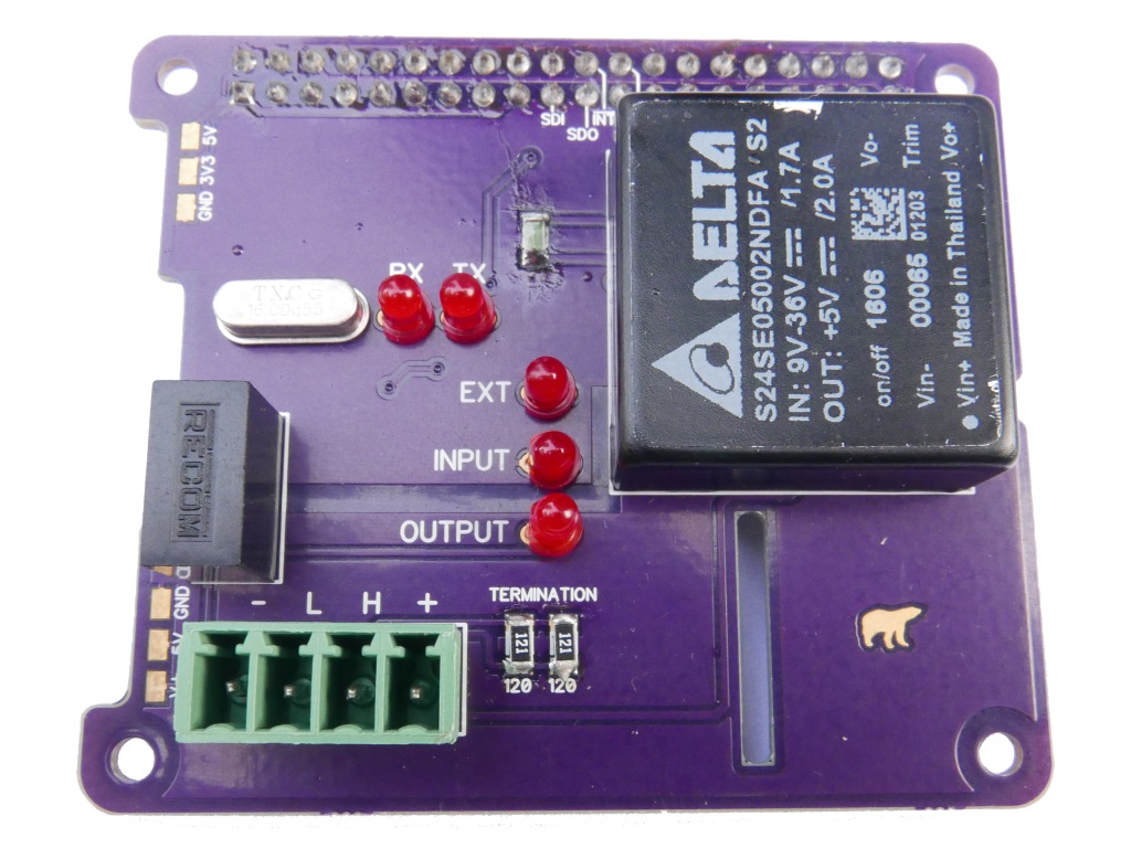
The very first one was noticed after I've already sent order to OSH Park. For back-powering isolation where 2 A are needed, I used the same footprint as for 100 mA DC-to-DC voltage regulator. There is no chance of getting a part that would support 2 A in such a small package. I've replaced it with properly sized 1x1" isolated voltage regulator and contacted OSH Park support. As my original order was not sent to fabrication facility yet, I got it swapped with a new design without any additional cost. OSH Park support rocks!
While waiting for a board, I continued going over the design and thus I've noticed I've forgotten to pull-up the reset line. Uncaught it would cause chip not to function so respin was definitely needed. Additionally I've changed layout of board a a bit alongside making a slightly bigger cuts to allow for official case to carry the board. I find it amusing that HATs made in accordance with official specification don't fit the official case. :)
What I didn't catch was that my new DC-to-DC brick needs a bit bigger holes. It was possible to get DC-to-DC converter in the board but with a lot of elbow grease. Definitely not what you would want. I also didn't notice I had damn pinout backward on one side of the chip. And guess what, since I've already sent for revision B to be manufactured, I couldn't change it before revision C.
I did try to mod-wire the revision A of the board but important traces to cut were under the DC-to-DC brick itself so there was no approaching them - not with tight drill holes I had. Fortunately I was able to jump the missing reset line and thus have a proof of concept all is working well.
Revision B arrived when I was already preparing for next revision due to already mentioned faults and thus I have just populated the "cheap" part of the board. It made no sense to mount $25 DC-to-DC voltage regulator if I know it is not going to work. Revision C did have few other changes to silk-screen and other minor changes. Most notable change, outside of DC-to-DC pinout correction, was changing EEPROM to be write protected when WP jumper was soldered over.
Original suggested EEPROM circuit makes write-protection to be default. This means you need to connect the jumper to write chip and then desolder it later to make it read-only. I find it much easier on me if all chips start with being writable and then you make solder bridge to make them read-only. Additionally, as chip has internal pull-up, this means you save a resistor. :)
As revision C came, all seemed great until I tried power-back circuit - it didn't work. Short troubleshooting later I've noticed my reading of remote on/off functionality was lacking a bit and thus I was missing connection of that pin to ground. With that single change power-back started working perfectly. Of course that meant revision D had to be made.
D? No issues what-so-ever. :)